
Competence Center for High-Resolution Superconducting Sensors (HSS) |
|

|
The Competence Center for High-Resolution Superconducting Sensors (HSS) is a worldwide unique facility for the development and (batch) fabrication of superconducting particle and radiation detectors with extremely high energy and time resolution, currently being established at KIT. The facility is operated in collaboration with the Institute for Data Processing and Electronics (IPE), the Institute of Micro- and Nanoelectronic Systems (IMS) and the partner institution Kirchhoff Institute for Physics at Heidelberg University. The goal of the center is to significantly increase production capacity for superconducting sensors, thereby enabling the development of large-scale experiments based on superconducting quantum sensors. The fabrication focuses on calorimetric low temperature particle detectors and superconducting electronics based on Josephson tunnel junctions, such as dc-SQUIDs or microwave SQUID multiplexers. To realize batch fabrication of these sensors, the equipment is designed for using 6-inch substrates and automated process control.
|
Overview of Production Machinery |
|
In the first stage of HSS, the production machinery consists of the following equipment:
|
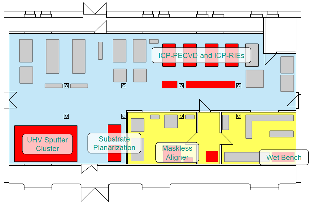
HSS at the Institute of Micro- and Nanoelectronic Systems (IMS) |
|||
|
The final location for HSS is the Karlsuhe Center for Optics and Photonics (KCOP). The HSS facility within KCOP has been optimally designed based on the fabrication systems and user requirements to ensure efficient and effective utilization of all machines. Since KCOP is expected to be completed in the first half of 2026, the HSS production machinery is currently being set up at its initial temporary installation site, the Institute of Micro- and Nanoelectronic Systems (IMS). A significant amount of the equipment has already been installed and is operational at KIT. In addition to purchasing the individual fabrication systems, all necessary manufacturing processes are currently being developed and optimized. Once the production machinery is relocated and the subsequent installation phase is completed, HSS will be immediately operational, as no major adjustments are expected for the already optimized processes. |
||
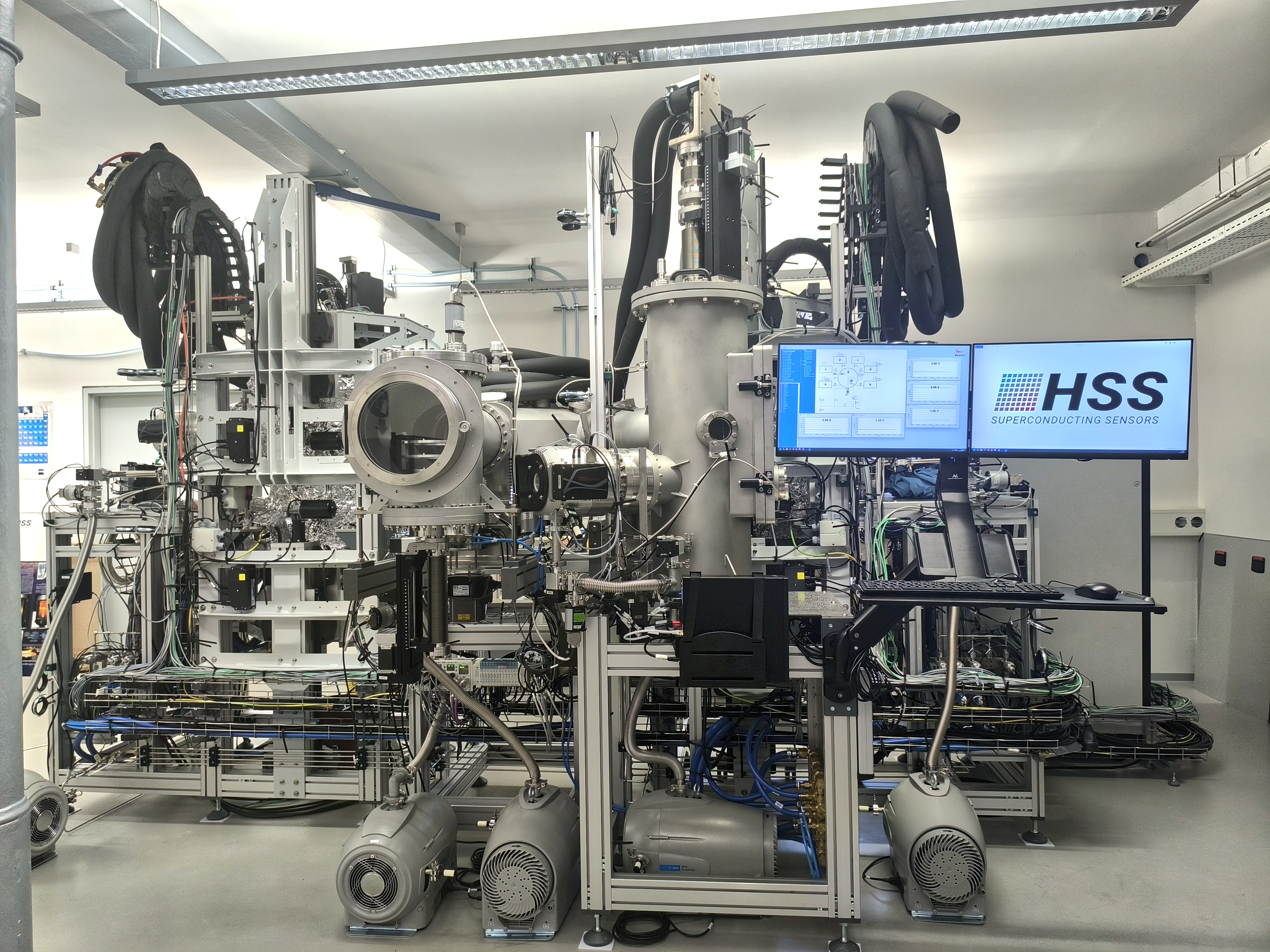
UHV Multi-Chamber Deposition System |
||
|
Operation PrincipleMagnetron sputtering is a physical deposition method in which ions generated in a plasma bombard a sputter target. The ejected atoms are then deposited onto a substrate.
Highlights
|
|
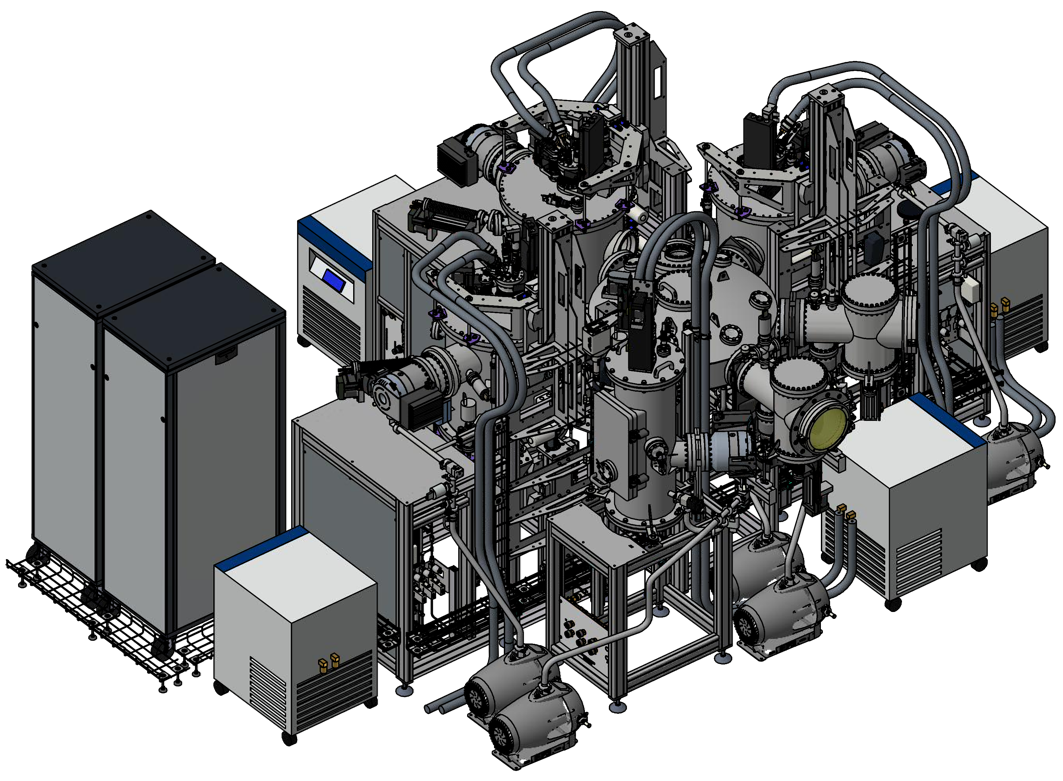
Upgrade for the UHV multi-chamber deposition system (planned for 2026) |
||
|
Operation PrincipleNew integrated coating method - electron beam evaporation: Heating and evaporation of target material by a focused electron beam with subsequent material deposition on a substrate surface
Highlights
|
|
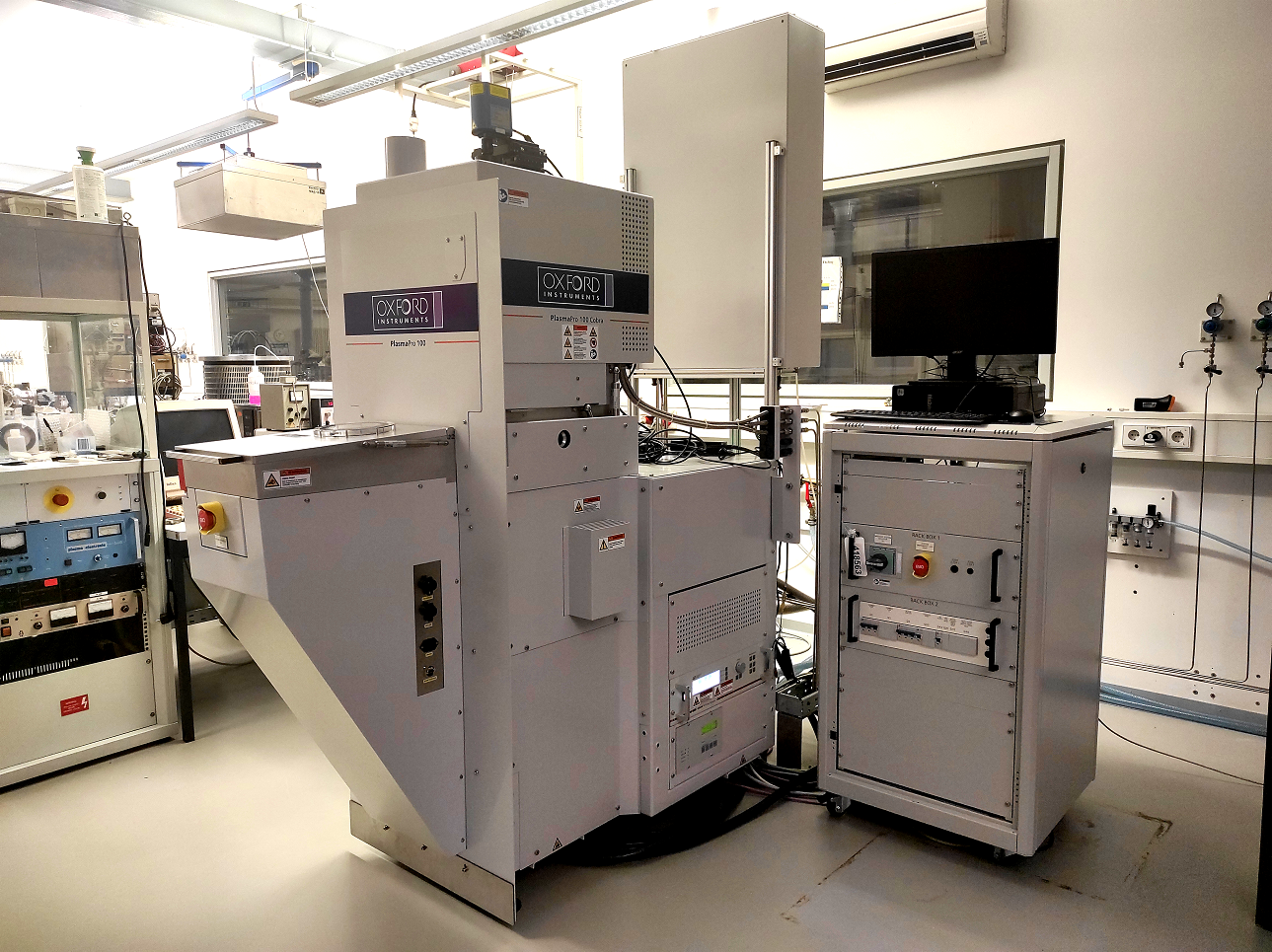
ICP-PECVD Deposition System |
||
|
Operation PrinciplePlasma-enhanced chemical vapor deposition of the insulators SiO2 and Si3N4 using monosilane and TEOS at low process temperatures of approx. 100 °C ensuring device compatibility.
Highlights
|
|
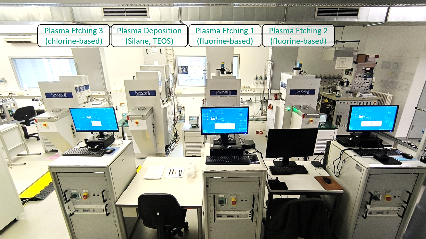
ICP-RIE Etching Systems |
||
|
Operation PrincipleAnisotropic dry etching process for various materials deposited on a substrate by chemical or physical etching using a fluorine- or chlorine-based plasma.
Highlights
|
|
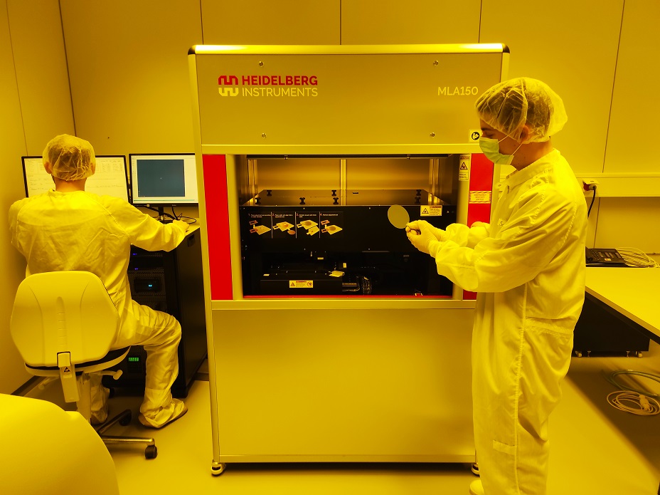
Direct-Writing Laser Lithography System |
||
|
Operation PrincipleDirect exposure of the design onto a photoresist-coated substrate using a 2D high-speed spatial light modulator and a 375 nm solid-state laser.
Highlights
|
|
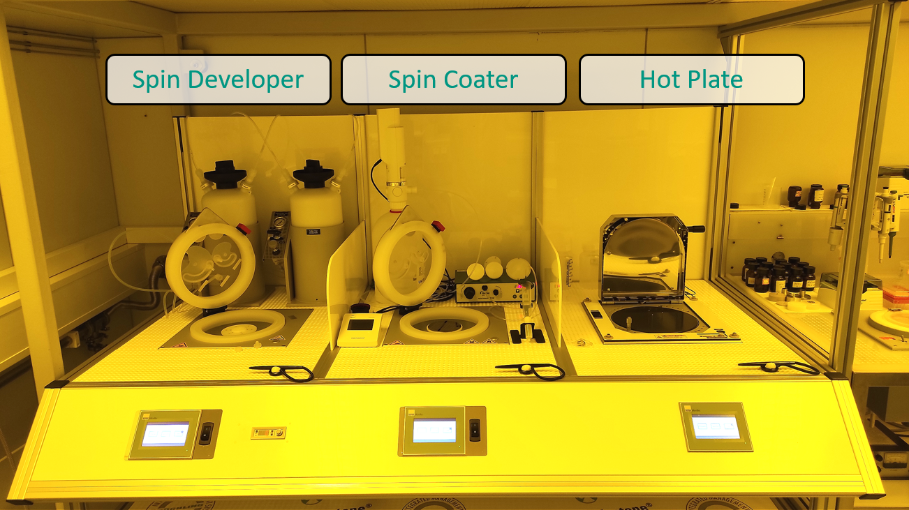
Customized Wet Bench for Photolithography Processes |
||
|
Operation PrincipleCustomized wet bench for photolithography processes, i.e. for resist coating of substrates, various baking processes and development after resist exposure.
Highlights
|
|